Shrinking Silicon
How Tech Hardware Got Microscopic
We completely take it for granted that the smartphone in your pocket is millions of times more powerful than the massive computers that sent humanity to the Moon. But if you open up a modern laptop, you’ll notice something mind-boggling: the actual components—the RAM modules, the processors, the storage—are smaller than a fingernail.
How did we manage to pack billions of electrical parts into a space smaller than a drop of water?
It wasn’t just a matter of making things smaller with a pair of tweezers; it required engineers to completely rewrite the rules of physics and chemistry. Here is how it's physically possible, along with a few wild facts that show just how crazy the engineering gets.
1. Printing with Extreme Lasers
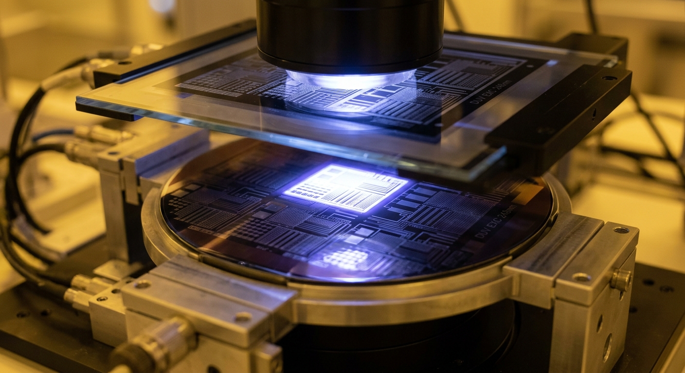
You can't build microchips using tiny mechanical tools; the components are simply too small. Instead, engineers print them using light. This process is called photolithography.
For decades, we used standard ultraviolet light to etch circuits onto silicon. But as we demanded smaller hardware, the light waves were too fat—it was like trying to paint a fine portrait with a giant house-painting brush.
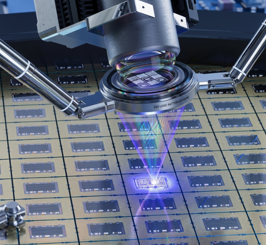
The Mind-Bending Fact: Today’s cutting-edge chips are built using EUV (Extreme Ultraviolet) light. To create this specific light, a high-power laser blasts a microscopic droplet of molten tin flying through a vacuum at 300 km/ph, vaporizing it into a tiny cloud of plasma that glows with the exact light needed.
The Easy View: Imagine using a laser so insanely sharp it can etch lines on a piece of silicon that are only a few atoms wide. Because our "paint brush" became a hyper-precise laser beam, the components shrunk to a fraction of their original size.
2. Building Skyscrapers on Silicon
For a long time, microchips were flat, like a single-story house. If you wanted more RAM or a bigger processor, you needed a larger piece of silicon to spread things out. Eventually, we simply ran out of physical space on the circuit boards.
So, chip architects shifted from expansive layouts to advanced 3D vertical stacking, similar to how urban architects build skyscrapers instead of suburban expansion.
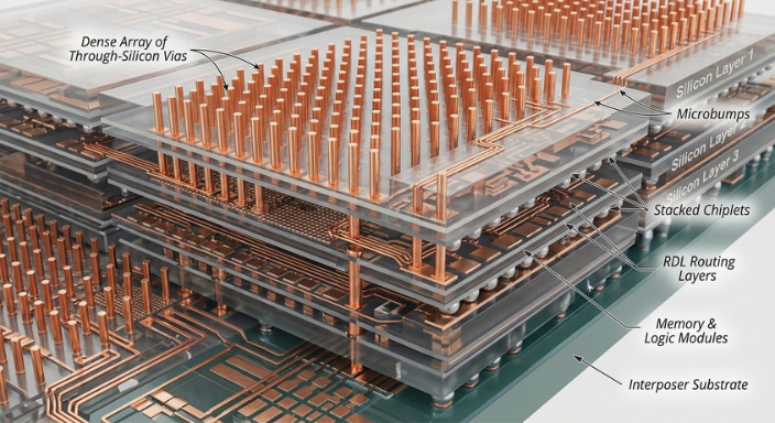
The Mind-Bending Fact: Modern memory (like the high-speed RAM and flash storage in your devices) relies on 3D stacking. Instead of placing memory cells side by side, manufacturers stack over 200 layers of memory cells vertically. To connect these layers, they drill microscopic vertical tunnels directly through the silicon, called TSVs (Through-Silicon Vias).
The Easy View: By stacking components vertically and wiring them straight through the floor and ceiling, we can pack terabytes of data into a tiny cube instead of a massive, flat board.
3. Stopping "Ghost" Electrons
As hardware shrunk to the size of just a few nanometers, engineers hit a terrifying wall governed by quantum physics: Quantum Tunneling.
When an electrical switch (a transistor) gets too small, the barrier separating the electricity becomes so thin that electrons literally turn into "ghosts." They teleport right through a closed gate, causing electricity to leak, wasting power, and melting the chip.
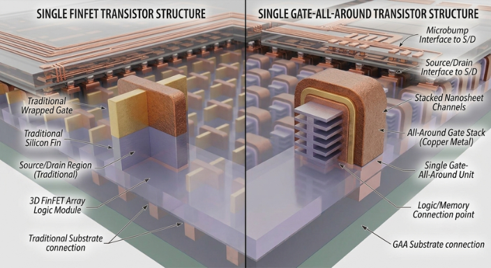
The Mind-Bending Fact: To stop this "ghostly" leakage, the industry invented Gate-All-Around (GAA) technology. Instead of a flat gate trying to stop the electricity, engineers broke the electrical path into a series of microscopic horizontal wires and completely wrapped the gate around them on all sides.
The Easy View: Think of it like trying to stop a leaky hose. A flat gate just presses down on one side, but a "Gate-All-Around" design acts like a tight fist wrapping completely around the hose, trapping the electrons and keeping the hardware incredibly small, stable, and power-efficient.
Your hardware is smaller today because we learned how to paint with extreme plasma light, stack circuits like high-rises, and build microscopic 3-D valves to stop electrons from teleporting.
The next time you look at a tiny stick of RAM or a memory card, remember: you aren’t just looking at plastic and metal. You're looking at billions of microscopic skyscrapers tamed by lasers and built at the absolute edge of human capability.
